Chapter 4 : AT89S8253 Microcontroller
- 4.1 AT89S8253 Microcontroller ID
- 4.2 Pin Description
- 4.3 AT89S8253 Microcontroller Memory Organisation
- 4.4 SFRs (Special Function Registers)
- 4.5 Watchdog Timer (WDT)
- 4.6 Interrupts
- 4.7 Counters and Timers
- 4.8 UART (Universal Asynchronous Receiver Transmitter)
- 4.9 SPI System (Serial Peripheral Interface)
- 4.10 Power Consumption Control
Introduction
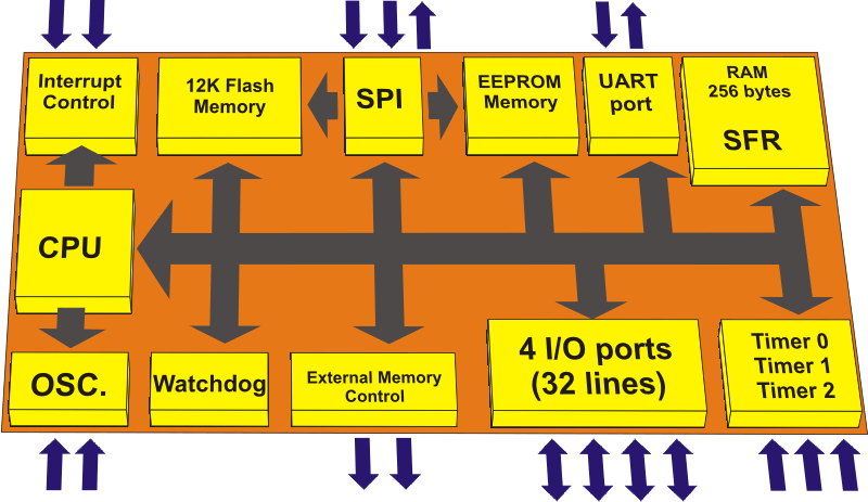
It has been more than 20 years since the first version of the 8051 microcontroller was launched. During that time it has undergone various upgrades and improvements. Today, the 8051 microcontroller is being manufactured across the globe by many manufacturers and under different names. Of course, the latest versions are by far more advanced than the original one. Many of them has the label “8051 compatible”, “8051 compliant”or “8051 family” in order to emphasize their “noble heritage”. These tags imply that microcontrollers have similar architecture and are programmed in a similar way using the same instruction set. Practically, if you know how to handle one microcontroller belonging to this family, you will be able to handle any of them. In other words, several hundreds of different models are at your disposal.
This book covers one of them called the AT89S8253, manufactured by Atmel. Why this particular one? Because it is widely used, cheap and uses Flash memory for storing programs. The last feature mentioned makes it ideal for experimentation due to the fact that program can be loaded and erased from it for many times. Besides, thanks to the built-in SPI System (Serial Programing Interface), the program can be loaded to the microcontroller even after embedding the chip in the target device.
4.1 The AT89S8253 microcontroller ID
- Compatible with 8051 family.
- 12Kb of Flash Memory for storing programs.
- Program is loaded via SPI System (Serial Peripheral Interface).
- Program may be loaded/erased up to 1000 times.
- 2Kb of EEPROM Memory.
- Power supply voltage: 4-6V.
- Operating clock frequency: 0-24MHz.
- 256 bytes of internal RAM for storing variables.
- 32 input/output pins.
- Three 16-bit timers/counters.
- 9 interrupt sources.
- 2 additional power saving modes (low-power idle and power-down mode).
- Programmable UART serial communication.
- Programmable watchdog timer.
- Three-level program memory lock
The AT89S53 comes in the following packages:
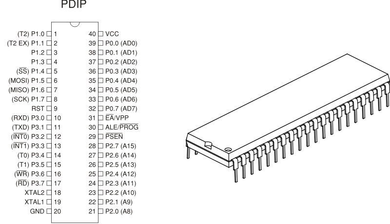
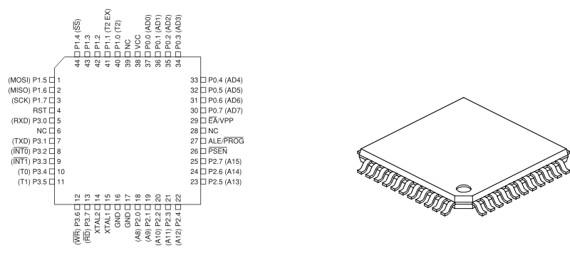
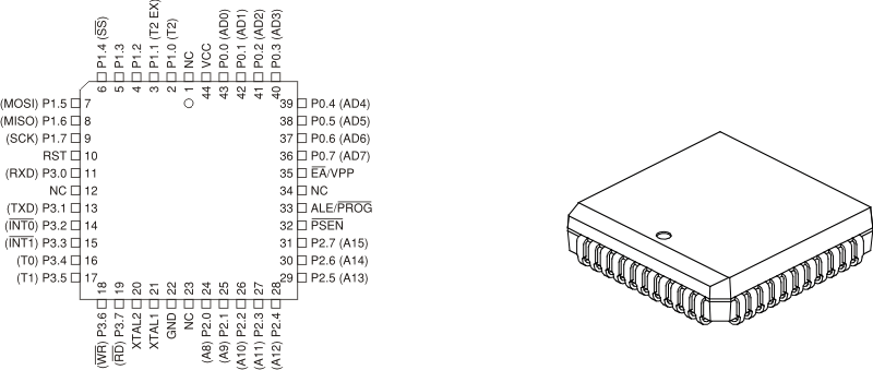
4.2 Pinout Description
VCC Power supply voltage (4-6V)
GND Ground ( Negative supply pole)
Port 0 (P0.0-P0.7) If configured as outputs, each of these pins can be connected to up to 8 TTL inputs. If configured as inputs, the pins can be used as high-impedance inputs as their potential is not defined relative to ground, i.e. they are floating. If additional (external) memory is used, these pins are used for accessing it. Signal on the ALE pin determines what and when will be transferred to this port.
Port 1 (P1.0-P1.7) If configured as outputs, each of these pins can be connected to up to 4 TTL inputs. When configured as inputs, these pins act as standard TTL inputs, that is, each of them is internally connected to the positive supply voltage via a resistor of relatively high impedance. Power supply voltage provided on these inputs is 5V. Also, the Port 1 pins have alternate functions as shown in the table below:
| PORT PIN | ALTERNATE FUNCTION |
|---|---|
| P1.0 | T2 (Timer 2 input) |
| P1.1 | T2EX (Timer 2 control input) |
| P1.4 | SS (SPI system control input) |
| P1.5 | MOSI (SPI system I/O) |
| P1.6 | MISO (SPI system I/O) |
| P1.7 | SCK (SPI system clock signal) |
Port 2 (P2.0-P2.7) Whether configured as an input or an output, this port acts the same as Port 1. If external memory is used, the high byte of the address (A8-A15) comes out on the Port 2 which is thus used for addressing it.
Port 3 (P3.0-P3.7) Similar to P1, Port 3 pins can be used as general inputs or outputs. They also have additional functions to be explained later in the chapter.
| PORT PIN | ALTERNATE FUNCTION |
|---|---|
| P3.0 | RXD (serial input) |
| P3.1 | TXD (serial output) |
| P3.2 | INT0 (external interrupt 0) |
| P3.3 | INT1 (external interrupt 1) |
| P3.4 | T0 (Timer 0 external input) |
| P3.5 | T1 (Timer 1 external input) |
| P3.6 | WR (External data memory write signal) |
| P3.7 | RD (External data memory read signal) |
RST Logic one (1) on this pin causes the microcontroller to be reset.
ALE/PROG In normal operation, the ALE pin is activated at a constant rate of 1/16 the oscillator frequency and can be used for external clocking and timing purposes. When external memory is used, a signal from this pin is used to latch the low byte of an address (A0-A7) from P0. During the process of writing a program to the microcontroller, this pin also serves as a control input.
PSEN This pin provides a signal used for accessing external program memory (ROM).
EA/VPP When this pin is connected to ground, the microcontroller reads program instructions from external program memory. If internal program memory is used, which is the common case, this pin should be connected to the positive power supply voltage (VCC). During the process of programming internal Flash mamory, this pin is supplied with +12V.
XTAL 1 This is internal oscillator input. It is used for the purpose of synchronizing the operation of the microcontroller with some other circuit or for connecting external oscillator when used.
XTAL 2 This pin is connected to internal oscillator output. Therefore, it is out of use when using external oscillator.
4.3 The AT89S8253 Microcontroller Memory Organization
Program Memory (ROM)
Program memory (ROM) with a capacity of 12Kb is designed in FLASH technology, which enables programs to be loaded and erased a large number of times. It is programmed via embedded SPI module (Serial Peripheral Interface). If necessary, it is possible to add external ROM memory chip, although 12Kb of ROM is usually more than enough.
Random Access Memory (RAM)
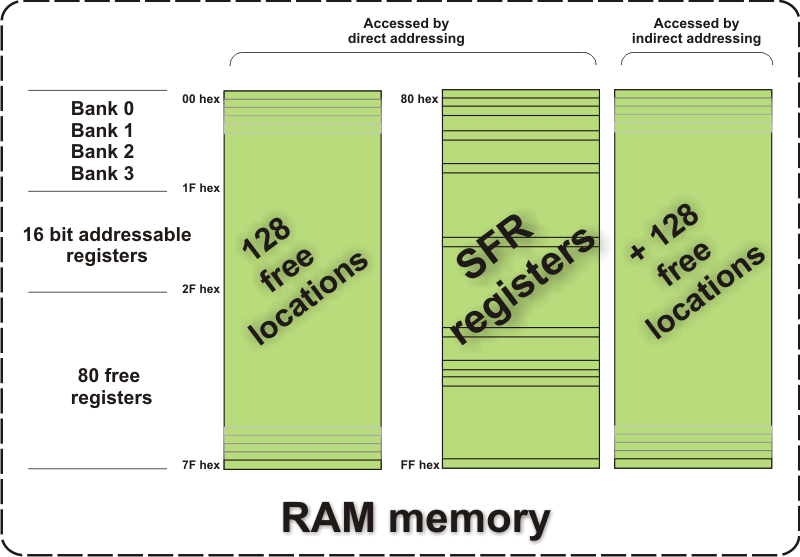
RAM memory consists of 3 blocks containing 128 registers each. Its structure falls into the 8051 standard:
- 128 general-purpose registers;
- 128 memory locations reserved for SFRs. Even though only some of them are trully used, free locations shouldn’t be used for storing variables; and
- 128 additional registers available for use (have no special purpose). Since they have the same addresses as SFRs, they are accessed by indirect addressing.
EEPROM Memory
EEPROM is a special type of memory having features of both RAM and ROM. The contents of the EEPROM may be changed during operation, but remains permanently saved even after the loss of power. The AT89S8253 microcontroller has in total of 2K of EEPROM, that is 2048 locations.
Memory Expansion
All mentioned above about ROM and RAM memory expansion remains in force when it comes to the AT89S8253 microcontroller as it is based on the 8051 core. In other words, both memories can be added as external chips with the capacity of up to 64Kb. The process of addressing is also the same as in the 8051 standard.
Types of addressing
Similar to all microcontrollers compatible with the 8051, there are two ways of addressing:
- Direct addressing (for example: MOV A,30h); and
- Indirect addressing (for example: MOV A,@R0).
4.4 Special Function Registers (SFRs)
The AT89S8253 microcontroller has in total of 40 Special Function Registers. For the sake of the compatibility with the previous 8051 models, the core registers (22 in total) are the same for all of them, while the others were added later for the purpose of controlling upgraded functions of the microcontroller.
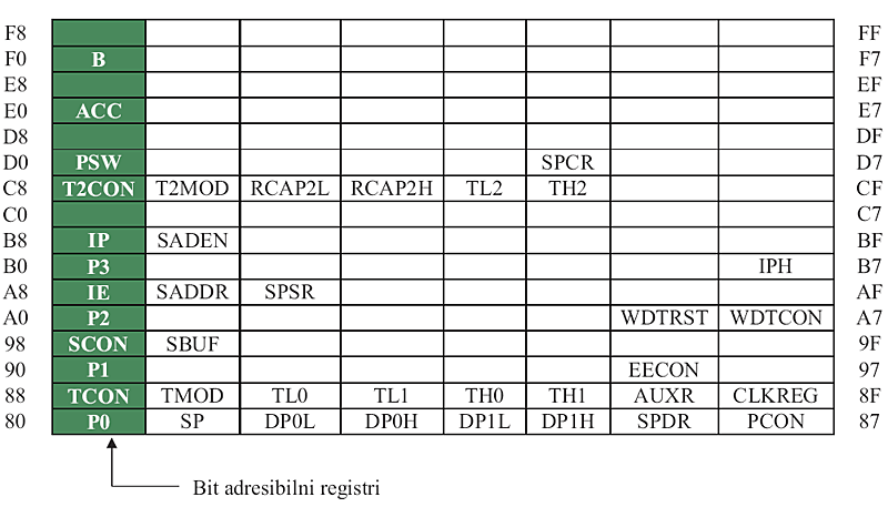
As shown in the table above, each of these registers has its name and specific address in RAM. Unoccupied locations are intended for the future upgraded versions of the microcontroller and shouldn’t be used. As their name suggests, these registers are mostly in control of one specific circuit within the microcontroller such as timers or SPI etc. and they will be discussed later in the book. This chapter covers only those SFRs controlling more than one circuit within the microcontroller.
Accumulator (ACC)
The accumulator, otherwise marked as ACC or A, belongs to the core registers of the 8051 microcontroller. Its contents is not modified.

B register
The B register also belongs to the core registers of the 8051 microcontroller. Bits of this register are not modified. It is used during multiply and divide operations (MUL and DIV instructions) to store the operands upon which these operations are performed.

PSW register (Program Status Word Register)
The PSW register belongs to the core registers of the 8051 microcontroller. Bits of this register are not modified.

SP registar (Stack Pointer Register)
The SP register belongs to the core registers of the 8051 microcontroller. Bits of this register are not modified.

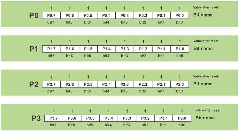
Registers P0, P1, P2, P3
Each bit of these registers corresponds to one of the port pins having the same name. These registers are therefore used for comminication with peripheral environment which is carried out by sending data from registers to the corresponding pins and vice versa. They belong to the core registers of the 8051 microcontroller and their bits are not modified.
R registers (R0 - R7)
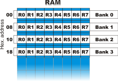
They belong to the core registers of the 8051 microcontroller. Their bits are not modified.
AUXR register (Auxiliary register)
The AUXR register contains only two active bits:

- DISALE
- 0 - ALE is activated at a constant rate of 1/6 the oscillator frequency.
- 1 - ALE is active only during execution of MOVX or MOVC instructions.
- Intel_Pwd_Exit
- 0 - When the microcontroller is in Power Down mode, the program proceeds with execution on high-to-low transition (1-0).
- 1 - When the microcontroller is in Power Down mode, the program proceeds with execution on low-to-high transition (0-1).
CLKREG register (Clock Register) X2
- 0 - The oscillator frequency (the XTAL1 pin) is divided by 2 before used as a clock (machine cycle lasts for 6 such periods).
- 1 - Quartz oscillator is used as a clock generator. This enables the quartz crystal of two times lower frequency (for example 6MHz instead of 12MHz) to be used for the same operating rate of the microcontroller.
Data Pointers
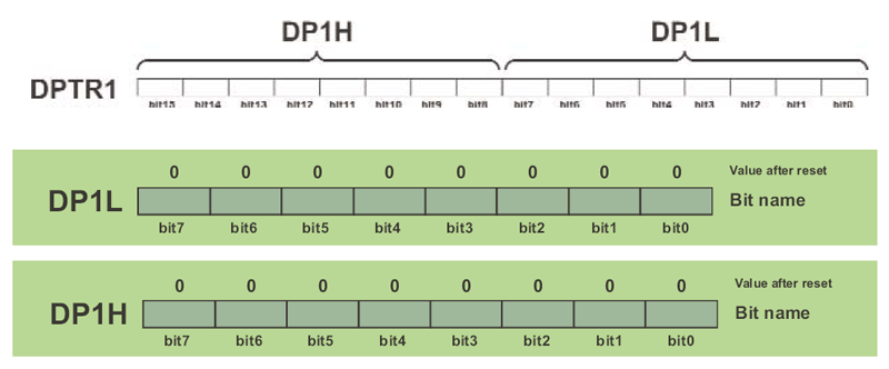
Data Pointers are not true registers as they don’t physically exist. They consist of two separate registers: DPH (Data Pointer High) and DPL (Data Pointer Low). All 16 bits are used for addressing external and internal EEPROM memory. The DPS bit of the EECON register determines the registers to be used as data pointers:
DPS=0 -> Data pointer consists of DP0L and DP0H registers and is marked as DPTR0.
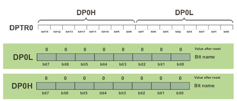
DPS=1 -> Data pointer consists of DP1L and DP1H registers and is marked as DPTR1.
Handling EEPROM memory
2 Kb of on-chip EEPROM memory enables this microcontroller to store data created during operation which must be permanently saved. In other words, all data stored in this memory remains permanently saved even after the loss of power. Minimum 100 000 writing cycles can be executed. This memory is easily used since there are only a few control bits enabling it.
EEPROM write and read is under control of the EECON special function register. Since the process of programming EEPROM is relatively slow (write to one register takes approximately 4mS), a small hardware trick is done in order to speed it up. When the EELD bit of the EECON register is set, the data is not directly written to the EEPROM registers, but loaded in a small buffer (temporary memory) with a capacity of 32 bytes. When this bit is cleared, the first data following it will be normally written to the EEPROM (takes 4 mS) along with all registers currently loaded in the buffer. Thus, it takes only 4mS to write all 32 bytes instead of 128mS otherwise required in a single byte writing.
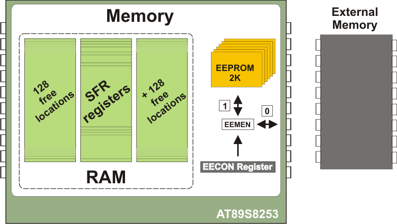
EEPROM memory is handled in the same way as external memory. For this reason, a special instruction for additional memory chip (MOVX) is also used for EEPROM write and read. The EEMEN bit of the EECON register determines whether the data is to be written/read from additional memory chip or on-chip EEPROM memory.
EECON register
Bits of the EECON register controls the operation of EEPROM memory:
WRTINH
The WRTINH bit is read-only. When the power supply voltage is too low for programming EEPROM, hardware automatically clears this bit, which means that write to EEPROM cannot be completed or is aborted if in progress.
RDY/BSY
The RDY/BSY bit is read-only.
- 0 - Write in progress (takes approximately 4mS).
- 1 - Write complete (data is written to EEPROM).
DPS
- 0 - Address for EEPROM write/read is stored in the DP0H and DP0L registers.
- 1 - Address for EEPROM write/read is stored in the DP1H and DP1L registers.
EEMEN
- 0 - Instruction MOVX is used for accessing external memory chip.
- 1 - Instruction MOVX is used for accessing internal EEPROM memory. If the register address is larger than 2K, the microcontroller will access external memory chip.
EEMWE
When set, the EEMWE bit enables write to EEPROM using the MOVX instruction. After completing EEPROM write, the bit must be cleared from within the program.
EELD
When set, the EELD bit enables up to 32 bytes to be written simultaneously. The bit is set and the MOVX instruction writes data to EEPROM (buffer is loaded). The bit is cleared before writing the last data. When the last MOVX is executed, the entire buffer is automatically loaded to EEPROM for 4mS.
4.5 Watchdog Timer (WDT)
The watchdog timer uses pulses generated by the quartz oscillator for its operation. It is disabled after reset and during Power Down Mode, thus having no effect on the program execution. If enabled, every time it counts up to the program end, the microcontroller reset occurs and program execution starts from the first instruction. Reset condition indicates that the program doesn’t work properly for some reason. The point is to prevent this from happening by setting instruction to reset the watchdog timer at the appropriate program location. Practically, the whole this process is in control of several bits of the WDTCON register.
Three bits (PS2, PS1 and PS0), which are in control of the prescaler, determine the most important feature of the watchdog timer- nominal time, i.e. time required to count up a full cycle.
The values contained in the table below are applied only when the 12MHz quartz oscillator is used.
| PRESCALER BITS | NOMINAL TIME | ||
|---|---|---|---|
| PS2 | PS1 | PS0 | |
| 0 | 0 | 0 | 16ms |
| 0 | 0 | 1 | 32ms |
| 0 | 1 | 0 | 64ms |
| 0 | 1 | 1 | 128ms |
| 1 | 0 | 0 | 256ms |
| 1 | 0 | 1 | 512ms |
| 1 | 1 | 0 | 1024ms |
| 1 | 1 | 1 | 2048ms |
WDTCON Register (Watchdog Control Register)
PS2,PS1,PS0
These three bits are in control of the prescaler and determine the nominal time of the watchdog timer. If the program doesn’t clear the WSWRST bit during that time, the watchdog timer will reset the microcontroller. When all three bits are cleared to 0, the watchdog timer has a nominal period of 16K machine cycles. When all three bits are set to 1, the nominal period is 2048K machine cycles.
WDIDLE
The WDIDLE bit enables/disables the watchdog timer in Idle mode:
- 0 - Watchdog timer is enabled in Idle mode (low-consumption mode).
- 1 - Watchdog timer is disabled in Idle mode.
DISRTO
The DISRTO bit enables/disables reset of peripheral circuits connected to the RST pin:
- 0 - Watchdog controls the state of the input reset pin. At the moment of reset, this pin acts for a moment as an output and generates a logic one (1). It causes the microcontroller and all other circuits connected to the RST pin to be reset.
- 1 - Reset triggered by the watchdog timer doesn’t affect the state of the reset pin. At the moment the watchdog timer resets the microcontroller, the reset pin remains configured as an input.
HWDT
The HWDT bit selects hardware or software mode for the watchdog timer:
- 0 - Watchdog is in software mode and can be enabled or disabled by the WDTEN bit.
- 1 - Watchdog is in hardware mode. To enable it, the sequence 1E/E1(hex) should be written to the WDTRST register. Only reset condition can disable the watchdog timer. In order to prevent the WCDT from resetting the microcontroller when the nominal time expires, the same sequence 1E/E1hex must be constantly repeated.
WSWRST
When set, this bit resets the watchdog timer in software mode (bit HWDT=0). In order to enable the microcontroller to operate without being interrupted, this bit must regularly be cleared from within the program. After being set, the watchdog timer is cleared by hardware, counting starts from zero and the bit is automatically cleared.
If the watchdog timer is in hardware mode, setting this bit has no effect on the watchdog timer operation.
WDTEN
The WDTEN bit enables/disables the watchdog timer in software mode (HWDT=0):
- 0 - Watchdog disabled.
- 1 - Watchdog enabled.
When the watchdog timer is in hardware mode (HWDT=1), this bit is read-only and reflects the status of the watchdog timer (whether it is enabled or disabled).

The WDTEN bit doesn’t clear the watchdog timer, it only enables/disables it. This means that the current state of the counter remains unchanged as long as WDTEN=0.
4.6 Interrupts
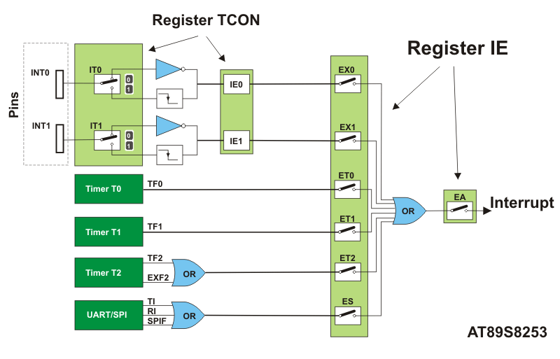
The AT89S8253 has in total of six interrupt sources, which means that it can recognize up to 6 different events that can interrupt regular program execution. Each of these interrupts can be individually enabled or disabled by setting bits of the IE register, whereas the whole interrupt system can be disabled by clearing the EA bit of the same register.
Since this microcontroller has embedded Timer T2 and SPI (they don't fall under the “8051 Standard”) which can generate an interrupt, it was necessary to make some changes in registers controlling interrupt system. Besides, there is a new interrupt vector (address 2B), i.e. program memory address from which the program proceeds with execution when the Timer T2 generates an interrupt. All these changes are made on the previously unused bits. This enables all programs written for the previous versions of the microcontrollers to be used in this one too without being modified. This is why the 8051-based microcontrollers are so popular.
IE register (Interrupt Enable Register)
EA bit enables or disables all interrupt sources (globally):
- 0 - disables all interrupts (even enabled).
- 1 - enables specific interrupts.
ET2 bit enables or disables Timer T2 interrupt:
- 0 - Timer T2 interrupt disabled.
- 1 - Timera T2 interrupt enabled.
ES bit enables or disables serial communication (UART and SPI) interrupts:
- 0 - UART and SPI interrupt disabled.
- 1 - UART and SPI interrupts enabled.
ET1 bit enables or disables Timer T1 interrupt:
- 0 - Timer T1 interrupt disabled.
- 1 - Timer T1 interrupt enabled.
EX1 bit enables or disables external interrupt through the INT0 pin:
- 0 - Interrupt on the INT0 pin disabled.
- 1 - Interrupt on the INT0 pin enabled.
ET0 bit enables or disables Timer T0 interrupt:
- 0 - Timer T0 interrupt disabled.
- 1 - Timer T0 interrupt enabled.
EX0 bit enables or disables external interrupt through the INT1 pin:
- 0 - Interrupt on the INT1 pin disabled.
- 1 - Interrupt on the INT1 pin enabled.
Interrupt Priorities
When several interrupts are enabled, it may happen that while one of them is in progress, another one is requested. In such situations, the microcontroller needs to know whether to proceed with the execution of current interrupt routine or to meet a new interrupt request. For this reason, there is a priority list on the basis of which the microcontroller knows what to do. The previous versions of the microcontrollers differentiate between two priority levels defined in the IP register.
As for the AT89S8253 microcontroller, there is an additional SFR register IPH which enables all the interrupts to be assigned 1 out of 4 priorities (excluding reset). Here is a list of priorities:
It is usually defined at the beginning of the program which one of the existing interrupt sources have high and which one has low priority level. According to this, the following occurs:
- If two interrupt requests, at different priority levels, arrive at the same time then the higher priority interrupt is always serviced first.
- If the both interrupt requests, at the same priority level, occur one after another, the one which came later has to wait until routine being in progress ends.
- If two interrupt requests of equal priority arrive at the same time then the interrupt to be serviced is selected according to the following priority list :
IP register (Interrupt Priority Register)

Bits of this register determine the interrupt source priority.
PT2 Timer T2 interrupt priority:
- 0 - Priority 0
- 1 - Priority 1
PS Serial port interrupt priority:
- 0 - Priority 0
- 1 - Priority 1
PT1 Timer T1 interrupt priority:
- 0 - Priority 0
- 1 - Priority 1
PX1 External interrupt INT1 priority:
- 0 - Priority 0
- 1 - Priority 1
PT0 Timer T0 interrupt priority:
- 0 - Priority 0
- 1 - Priority 1
PX0 External interrupt INT0 priority:
- 0 - Priority 0
- 1 - Priority 1
IPH Register (Interrupt Priority High)

PT2H Timer T2 interrupt priority
PSH Serial port interrupt priority
PT1H Timer T1interrupt priority
PX1H External interrupt INT1 priority
PT0H Timer T0 interrupt priority
PX0H External interrupt INT0 Priority
Bits of this register can be combined with appropriate bits of the IP register. This is how a new priority list with 4 interrupt priority levels (5 including reset) is obtained.
| IP BIT | IPH BIT | INTERRUPTS |
|---|---|---|
| 0 | 0 | Priority 0 (lowest) |
| 0 | 1 | Priority 1 (low) |
| 1 | 0 | Priority 2 (high) |
| 1 | 1 | Priority 3 (highest) |
Processing interrupt
When an interrupt request arrives, the microcontroller automatically detects the interrupt source and the following occurs:
| INTERRUPT SOURCE | JUMP ADDRESS |
|---|---|
| IE0 | 3h |
| TF0 | Bh |
| IE1 | 13h |
| TF1 | 1Bh |
| RI, TI, SPIF | 23h |
| TF2, EXF2 | 2Bh |
| All addresses are in hex format | |
Appropriate subroutines processing interrupts are stored at these addresses. Instead of them, there are usually jump instructions specifying locations at which these subroutines reside.
4. When an interrupt routine is executed, the address of the next instruction to be executed is popped from the stack to the program counter and the program proceeds from where it left off.
4.7 Counters and Timers
Timers T0 and T1
The AT89S8253 has three timers/counters marked as T0, T1 and T2. Timers T0 and T1 completely fall under the 8051 Standard. There are no changes in their operation.
Timer T2
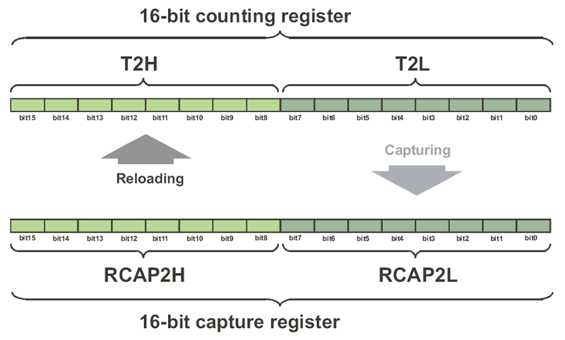
Timer 2 is a 16-bit timer/counter installed only in new versions of the 8051 family. Unlike timers T0 and T1, this timer consists of 4 registers. Two of them, TH2 and TL2, are connected serially in order to form a larger 16-bit timer register. Like timers 0 and 1, it can operate either as a timer or as an event counter. Another two registers, RCAP2H and RCAP2L, are also serially connected and operate as capture registers. They are used to temporarily store the contents of the counter register.
The main adventage of this timer compared to timers 0 and 1 is that all read and swap operations are easily performed using one instruction. Similar to T0 and T1, it has four different modes of operation to be described later in this chapter.
T2CON (Timer/Counter 2 Control Register)
This register contains bits controlling the operation of timer 2.
TF2 bit is automatically set on timer 2 overflow. In order to detect the next overflow, this bit must be cleared from within the program. If bits RCLK and TCLK are set, overflow has no effect on the TF2 bit.
EXF2 bit is automatically set when a capture or a reload is caused by a negative transition on the T2EX pin. It generates an interrupt (if enabled), unless the DCEN bit of the T2CON register is set. The EXF2 bit must be cleared from within the program.
RCLK is receive clock bit which determines which timer is to be used as receive clock for serial port:
- 1 - T2 is used as receive clock for serial port.
- 0 - T1 is used as receive clock for serial port.
TCLK is transmit clock bit which determines which timer is to be used as transmit clock for serial port:
- 1 - T2 is used as transmit clock for serial port.
- 0 - T1 is used as transmit clock for serial port.
EXEN2 is timer 2 external enable bit used to include the T2EX pin in timer 2 operation:
- 1 - Signal on the T2EX pin affects timer 2 operation.
- 0 - Signal on the T2EX pin is ignored.
TR2 is timer 2 run control bit used to enable/disable timer 2:
- 1 - Timer 2 enabled.
- 0 - Timer 2 disabled.
C/T2 is timer/counter 2 select bit used to select pulses to be counted by counter/timer 2:
- 1 - 16-bit register (T2H and T2L) counts pulses on the C/T2 pin (counter).
- 0 - 16-bit register (T2H and T2L) counts pulses from the oscillator (timer).
CP/RL2 is timer 2 capture/reload bit used to define transfer direction:
- 1 - If EXEN=1, pulse on the T2EX pin will cause a number to be transferred from counter to capture register.
- 0 - Under the same condition, signal on the T2EX pin will cause a number to be transferred from capture to counter register.
Timer T2 in Capture mode
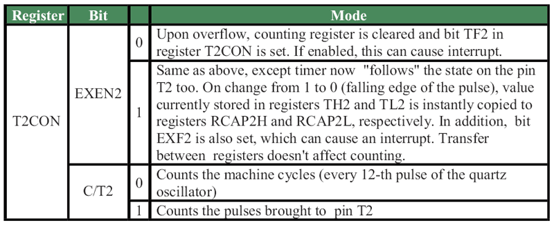
If the CP/RL2 bit of the T2CON register is set, timer 2 operates according to the figure below. This is so called Capture mode in which the value of the counter register (consisting of RCAP2H and RCAP2L) can be “captured” and copied to the capture register (consisting of RCAP2H and RCAP2L), thus not affecting the counting process. This is how it operates:
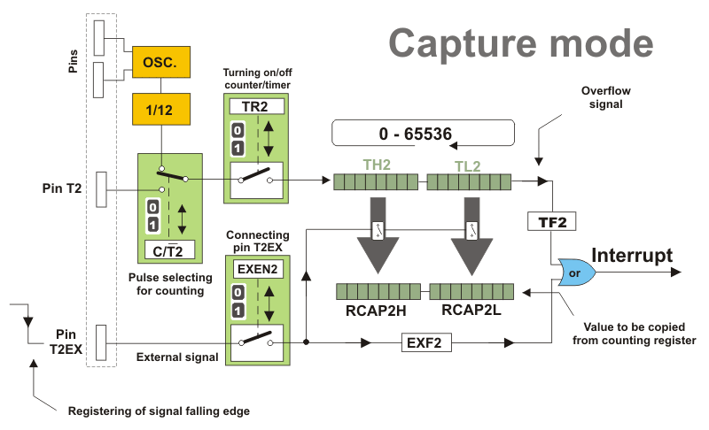
Settings:
Timer T2 in auto-reload mode
The auto-reload mode configures timer 2 as a 16-bit timer or event counter with automatic reload. It is controlled by the DCEN bit of the T2MOD register. Setting the DCEN bit enables timer 2 to count up or down from the specified value. The T2EX pin controls the counting direction:
T2OE - Enables timer 2 to operate as independent clock generator.
DCEN - When set, it enables counting in either direction- "up" and "down".
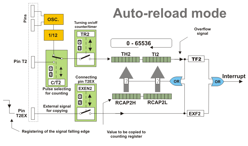
As seen in figure above, unlike Capture mode, the contents of the capture register (RCAP2H, RCAP2L) is now copied in the opposite direction upon an overflow occurs, from capture (RCAP2H, RCAP2L) to counter register (TH2, TL2).
Settings of Auto Reload mode are shown in the table below:
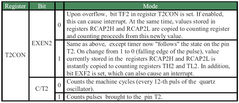
All previously mentioned about timer 2 is in force only if the T2MOD register hasn't been changed, i.e. if DCEN = 0. Otherwise, timer/counter is enabled to count in either direction, which depends on the T2EX pin:
T2EX = 0 Timer 2 counts down
T2EX = 1 Timer 2 counts up
T2EX = 1 Timer 2 counts up
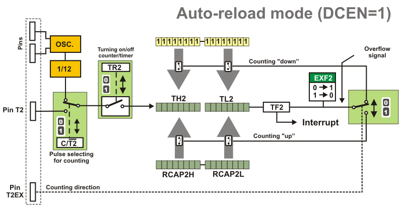
On counting up, the whole procedure is similar to the previous mode with one exception referring to the function of the EXF2 bit.
On counting down, an overflow occurs when values stored in the counter and capture registers match. It causes the TF2 bit as well as all bits of registers T2H and T2L to be set while the counter keeps on counting down: 65535, 65534,65533...
In either case, the EXF2 bit is assigned a new function. When an overflow occurs, this bit inverts the signal and cannot be used for generating an interrupt anymore. Instead, it serves as supplementary bit (the 17th bit) of the counter register, making this counter virtually a 17-bit register.
Timer T2 as a baud rate generator
The Timer T2 can be used as a baud rate generator and a clock generator simultaneously. If the RCLK or TCLK bit of the register TCON is set, timer T2 turns into a clock generator, so called Baud Rate generator). This mode is very similar to auto-reload mode. The baud rate is computed using the following formula:

There are a few details to be aware of:
Timer T2 as a clock generator
As previously mentioned, timer T2 can also be used as a clock generator. In all previous examples, the P1.0 pin (marked as T2 in figures) is used as an alternative clock generator for this timer, i.e. it acts as an input. Besides, it can also output pulses. By using a 16MHz quartz crystal, the frequency of pulses it generates ranges from 61Hz to 4MHz with a 50% duty-cycle.
To configure this pin as an output, the C/T2 bit of the T2CON register must be cleared, whereas the T2OE bit of the T2MOD register must be set. The TR2 bit enables the timer and the pin outputs rectangular waves the frequency of which ca be calculated using the formula below:

4.8 Universal Asynchronous Receiver Transmitter (UART)
The Universal Asynchronous Receiver Transmitter (UART) has the same features as that of the standard 8051 microcontrollers. It means that it can operate in 1 out of 4 different modes, which is controlled by bits SM0 and SM1 of the SCON register.
Multiprocessor Communication
Multiprocessor communication (the SM2 bit of the SCON register is set) enables automatic address recognition by allowing the serial port to examine the adress of each incoming command. The process of writing a program is much easier therefore as the microcontrollers sharing the same interface don't have to check each address received via the serial port. Let's make it clear.
Two special function registers, SADDR and SADEN, enable multiprocessor communication. Each device has an individual address that is specified in the SADDR register, while the so called mask address is written to the SADEN register. The mask address contains don't care bits which provide the flexibility to address one or more slaves at a time. In other words, it defines which bits of the SADDR register are to be used and which are to be ignored.

When the master wants to transmit data to one of several slaves, it first sends out an address byte which identifies the target device. An address byte differs from a data byte in that the 9th bit is 1 in an address byte and 0 in a data byte. After receiving the address byte, all slaves check whether it matches their address. The adressed slave clears its SM2 bit and prepares to receive the data bytes to come. The slaves that weren't addressed leave their SM2 bits set and ignores the coming data bytes.
The most simple example is a “mini-network” comprising only 3 microcontrollers:
Microcontroller A is the master and communicates with devices “B” and “C”.
Microcontroller B: SADDR = 1100 0000
                   SADEN = 1111 1101
                 Address = 1100 00X0

Microcontroller C: SADDR = 1100 0000
                   SADEN = 1111 1110
                 Address = 1100 000X
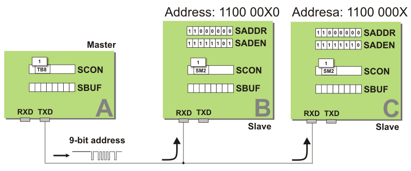
Although both microcontrollers B and C are assigned the same address (1100 0000), the mask in register SADEN is used to differentiate between them. It enables the master to communicate with both of them separately or at the same time:
If transmit address is 1100 0010, the data will be sent to slave device B.
If transmit address is 1100 0001 the data will be sent to slave device C.
If transmit address is 1100 0000 the data will be sent to both slave devices.
If transmit address is 1100 0001 the data will be sent to slave device C.
If transmit address is 1100 0000 the data will be sent to both slave devices.
4.9 SPI System (Serial Peripheral Interface)
In addition to UART system, the AT89S8253 has also another system for serial communication which doesn’t fall into the 8051 Standard. It is SPI system which provides a high-speed synchronous data transfer between the microcontroller and one or more peripheral devices or between multiple microcontrollers. Here, one microcontroller is always considered main and is called master therefore. It defines rate, transfer direction (whether data is to be transferred or received) and data format. The other is slave device which is in subordinated position, which further means that it cannot start data transfer, but has to adjust to conditions set by the master device.
The data are transferred via full duplex connection using 3 conductors connected to pins MISO (P1.6), MOSI (P1.5) and SCK (P1.7). The forth pin-control pin SS- is not used on the master side and may be used as a general-purpose input/output therefore, while on the slave side it must have voltage level 0. When the SS pin on the slave side is set, its SPI system is deactivated and the MOSI pin can be used as a general-purpose input.
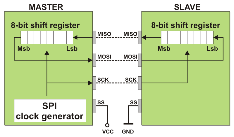
As shown on the schematic, pins MISO and MOSI are configured differently in the master and slave device (as inputs or outputs), which is determined by the MSTR bit of the SPCR register.

Knowing abbraviations makes connection easier:
MISO - master in, slave out; MOSI - master out, slave in; SCK - serial clock; SS - slave select;
MISO - master in, slave out; MOSI - master out, slave in; SCK - serial clock; SS - slave select;
Similar to many other circuits within the microcontroller, the SPI system can also be configured to operate in several modes.
Normal SPI mode (buffer out of use)
Data written to the SPI data register SPDR is automatically transferred to an 8- bit shift register. SPI clock generator is enabled and serial data appears on the MOSI pin. An initial delay may occur for the sake of synchronization with the main oscillator.
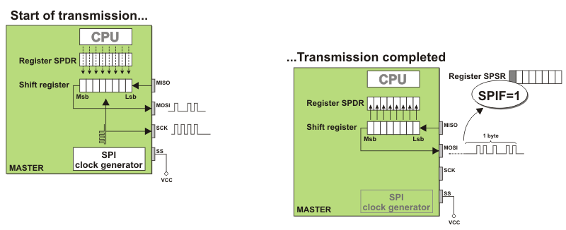
After sending one byte, the SPI clock generator stops, the SPIF bit (flag) is set, the received byte is transferred to the SPDR register and, if enabled, an interrupt is generated.
Any attempt to write another byte to the SPDR register while byte transmit is in progress will cause the WCOL bit to be set. It indicates that an error has occured. However, the byte will be succesfully transmitted, while the new byte will be ignored, i.e. it will not be transmitted.
Enhanced SPI mode (buffer in use)
Enhanced mode is similar to normal except that this time data goes through one more register while being transmitted. It makes no sense at first sight, but communication is really faster. Look at the figure below...
Data written to the SPI data register SPDR is automatically transferred to the capture register (buffer), which causes the WCOL bit to be set. It means that the buffer is full and any further write will cause an overflow. Control electronics (hardware) cleares this bit after transmitting data from buffer to the shift register and after commencing serial data transmit. If the byte sent is the first, the data is immediately transmitted to the shift register (still empty), thus clearing the WCOL bit (buffer is empty).
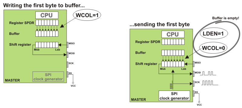
While one byte transmit is in progress, the next byte to transmit may be written to the SPDR register. It will be immediately moved to buffer. In order to check whether data transmit is in progress, it is sufficient to check the logic state of the LDEN bit of the SPSR register. If this bit is set (Load Enable) and the WCOL bit is cleared, data transmit is in progress and buffer is empty so the next byte can be written to the SPDR register.
How to select the right mode? If individual bytes are sent occasionally then there is no need to complicate- the best solution is the normal mode. If it is necessary to send a great amounts of data, it is better to use enhanced mode in which the clock oscillator is enabled as far as buffer is regularly loaded and the WCOL bit is set. In addition, no time is needed for synchronization and data is easily and efficiently transferred.
The SPI system is under control of 3 special function registers. These are SPDR, SPSR and SPCR.
SPDR (SPI Data Register)
The SPDR register is used for storing data to be transferred via SPI (in serial format). It is also used for storing received data.
SPSR (SPI Status Register)
SPIF Interrupt flag. Upon data transfer, this bit is automatically set and an interrupt is generated if SPIE=1 and ES=1. The SPIF bit is cleared by reading SPSR followed by reading/writing SPDR register.
WCOL This bit is set in normal mode (ENH=0) if the SPDR register is written during data transfer is in progress. The write is premature and has no effect. It is called Write Collision. This bit is cleared in the same manner as the SPIF bit.
The bit is set in enhanced mode (ENH=1) when buffer is full. It is indication that a new data is ready to be transmitted to the shift register.
The bit is set in enhanced mode (ENH=1) when buffer is full. It is indication that a new data is ready to be transmitted to the shift register.
In enhanced mode, a new data can be written to buffer when the WCOL bit is set. In addition, the WCOL bit must be cleared.
DISSO When set, this bit causes the MISO pin to float, thus enabling several slave microcontrollers to share the same interface. Normally, the first byte, called address byte, is received by all of them, but only one should clear its DISSO bit.
ENH
0 SPI system operates in normal mode (without buffer).
1 SPI system operates in enhanced mode.
0 SPI system operates in normal mode (without buffer).
1 SPI system operates in enhanced mode.
SPCR (SPI Control Register)
SPIE When this bit is set, the SPI system can generate an interrupt.
SPE This bit enables SPI communication. When set, pins SS, MOSI, MISO and SCK are connected to the microcontroller pins P1.4, P1.5, P1.6 and P1.7.
DORD Bit determines which bytes in serial communication are to be sent first:
- 0 - MSB bit is sent first.
- 1 - LSB bit is sent first.
MSTR Bit determines whether the microcontroller is to operate as master or slave:
- 0 - Operate as slave.
- 1 - Operate as master.
CPOL Bit controls the SCK pin logic state when the SPI communication is not in progress:
- 0 - Pin SCK is cleared.
- 1 - Pin SCK is set.
CPHA This bit along with the CPOL bit controls relation between clock and data in serial format. Refer to the figure below.
SPR1,SPR0 When SPI system operates as master, these two bits determine boud rate, i.e. clock signal frequency of the master device. When operates as slave, these bits have no effect and SPI system operates at a rate imposed by the master device.
| SPR1 | SPR0 | SCK |
|---|---|---|
| 0 | 0 | Fosc/4 |
| 0 | 1 | Fosc/16 |
| 1 | 0 | Fosc/64 |
| 1 | 1 | Fosc/128 |
Serial data format if CPHA=0
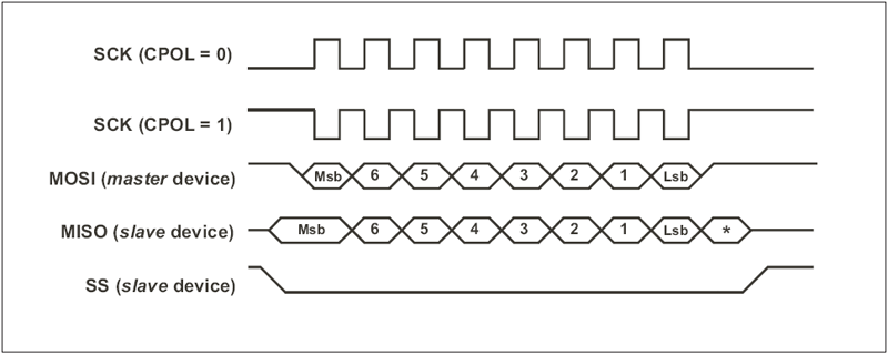
* not defined. It is usually MSB of previously received byte.
Serial data format if CPHA=1
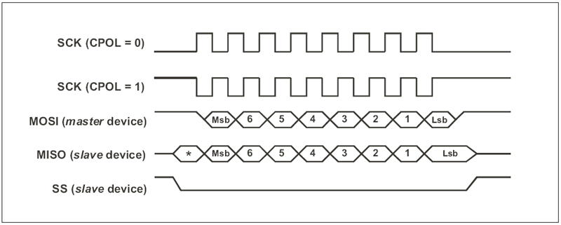
* not defined. It is usually LSB of previously received byte.
Two things are important to remember when configuring SPI system:
- Master should be configured before slave.
- When writing bits to the SPCR register, the SPE bit enabling SPI should be set last, i.e. after setting all other parameters.
4.10 Power Consumption Control
Like all models belonging to the 8051 series, this microcontroller can operate in 1 out of 3 modes: normal (consumption ca. 25 mA), Idle(consumption ca. 6.5 mA) and Power Down (consumption ca. 40 uA). The mode of operation is selected by bits of the PCON register (Power Control Register). Three bits are changed compared to the basic model:
PCON register
The purpose of the bits of the PCON register:
SMOD1 When set, this bit makes boud rate twice as high.
SMOD0 Bit determines the purpose of the 7th bit of the SCON register:
- 0 Seventh bit of the SCON register has the function of SM0, i.e. selects mode of operation.
- 1 Seventh bit has the function of FE, i.e. detects errors. It is rarely used.
POF Bit is automatically set when the voltage level reaches maximum (must be higher than 3V) after powering on. It is used for detecting cause for reset (power on or restart condition after exiting Power Down mode).
GF1 General purpose bit (available for use).
GF0 General purpose bit (available for use).
PD By setting this bit, the microcontroller is set in Power Down mode.
IDL By setting this bit, the microcontroller is set in Idle mode.
When something goes wrong...
If something unexpected happens during the operation of the microcontroller, what most bothers is the fact that it’s never the microcontroller's fault. Although it’s not self-evident, the microcontroller always obediently follows program instructions. For this reason, it is necessary to pay special attention to several “critical points” when writing a program. The first one is RAM memory.
Even though it is designed to meet needs of the majority of users and has all required, a memory space intended for RAM is still only a single entity. It means that there are no phisically separated registers R0-R7, general purpose registers, stack etc. Instead, these are differently designated parts of the same “memory shelf”. Refer to the figure below.
If we neglect this “detail”, there is a risk that the program suddenly starts to perform unpredictably. In order to prevent it, it is necessary to take care of the following:
If only registers R0-R7 from bank 0 are in use, everything is easily kept under control and program memory locations from 08h to 1Fh are available for use. If registers, otherwise having the same names, from some other bank are in use, you should be careful when using locations whose addresses are less than 20h because it can cause “R” registers to be erased.
If bit-variables are not used in the program, program memory locations 20h-2Fh are available for use. If the program contains bit-variables, you should be careful when using these location in order not to change them accidentaly.
By default, the data pushed onto stack occupy program memory locations starting from 08h. If the banks 1, 2 or 3 are in use, their contents will be certainly erased. For this reason, it is recommended to set the Stack Pointer value to be greater than 20h or even greater at the beginning of the program.
SFRs are used for controlling the microcontroller operation. Each of them has its specific purpose and it should be observed. It means that they cannot be used as general purpose registers even in the event that some of their locations is not occupied.
Instruction set, recognized by the microcontroller, contains instructions which can be used for controlling individual bits of registers at program memory location 20h-7Fh. Besides, individual bits of some SFRs (not all of them) can also be directly accessed. Addresses of these registers are divisible by 8.
If memory is expanded by adding external RAM or ROM memory chip, ports P0 and P2 are not available for use regardless of how many pins are actually used for memory expansion.
The DPTR register is a 16-bit register comprised of registers DPH and DPL which are 8-bit wide each. The DPTR register should be considered like that practically. For example, when pushing it onto the Stack, DPL should be pushed first, then DPH.
When used, serial communication is under control of the SCON register. Besides, registers TCON and TMOD should be configured for this purpose as well since the timer T1 is mostly used for boud rate generation.
When some of the interrupts is enabled, you should be careful because there is a risk that program starts to perform unexpectedly. When an interrupt request arrives, the microcontroller will execute instruction in progress, push the address of the first following location onto the stack (in order to know from where to continue) and jump to the specified interrupt routine address. When the routine has been executed, the microcontroller will pop the address from the stack and continue from where it left off. However...
The microcontroller saves only the address to continue from after routine execution. What is usually neglected is the fact that the contents of many registers can be changed during routine execution. The program normally procedees with execution considering the changed registers correct if their original vaules haven't been saved, thus causing a total chaos. The worst thing is that this problem can be manifested anytime: at the moment or several days later (depending on the moment an interrupt occurs). Obviously, the only solution is to save the state of all important registers at the beginning of interrupt routine and to update these values before returning to the program. We are actually talking about the following registers:
- PSW
- DPTR (DPH, DPL)
- ACC
- B
- Registers R0 - R7
Note: Contents of registers are usually saved by being pushed onto the Stack using the PUSH instruction. However, instructions such as “PUSH R0” cannot be used here because the microcontroller “doesn’t know” which register is concerned as there are 4 banks with registers haing the same names R0-R7. For this reason, it is necessary to save addresses of these registers instead of their names using the PUSH 00h instruction.
When some of the instructions for indirect addressing is used, you should be careful not to use them for accessing SFRs as the microcontroller ignores their addresses and accesses free RAM locations having the same addresses as SFRs.
When UART system for serial communication is used, setting bits RI and TI of the SCON register generated the same interrupt. If such an interrupt is generated, it is first necessary to detect interrupt source (byte is sent, received or both). It is important to remember that the microcontroller only sets these bits so that they must be cleared from within the program. Otherwise, the program gets stuck and executes the same interrupt routine over and over again.
A list of bit-addressable registers
Accumulator (Address: E0)
| ACC | ||||||||
|---|---|---|---|---|---|---|---|---|
| After reset | 0 | 0 | 0 | 0 | 0 | 0 | 0 | 0 |
| Bit name | - | - | - | - | - | - | - | - |
| Bit address | E7 | E6 | E5 | E4 | E3 | E2 | E1 | E0 |
B register (Address: F0)
| B | ||||||||
|---|---|---|---|---|---|---|---|---|
| After reset | 0 | 0 | 0 | 0 | 0 | 0 | 0 | 0 |
| Bit name | - | - | - | - | - | - | - | - |
| Bit address | F7 | F6 | F5 | F4 | F3 | F2 | F1 | F0 |
Interrupt Priority register (Address: B8)
| IP | ||||||||
|---|---|---|---|---|---|---|---|---|
| After reset | X | X | 0 | 0 | 0 | 0 | 0 | 0 |
| Bit name | - | - | PT2 | PS | PT1 | PX1 | PT0 | PX0 |
| Bit address | BF | BE | BD | BC | BB | BA | B9 | B8 |
Interrupt Enable register (Address: A8)
| IE | ||||||||
|---|---|---|---|---|---|---|---|---|
| After reset | 0 | X | 0 | 0 | 0 | 0 | 0 | 0 |
| Bit name | EA | - | ET2 | ES | ET1 | EX1 | ET0 | EX0 |
| Bit address | AF | AE | AD | AC | AB | AA | A9 | A8 |
Port 0 (Address: 80)
| P0 | ||||||||
|---|---|---|---|---|---|---|---|---|
| After reset | 1 | 1 | 1 | 1 | 1 | 1 | 1 | 1 |
| Bit name | - | - | - | - | - | - | - | - |
| Bit address | 87 | 86 | 85 | 84 | 83 | 82 | 81 | 80 |
Port 1 (Address: 90)
| P1 | ||||||||
|---|---|---|---|---|---|---|---|---|
| After reset | 1 | 1 | 1 | 1 | 1 | 1 | 1 | 1 |
| Bit name | - | - | - | - | - | - | - | - |
| Bit address | 97 | 96 | 95 | 94 | 93 | 92 | 91 | 90 |
Port 2 (Address: A0)
| P2 | ||||||||
|---|---|---|---|---|---|---|---|---|
| After reset | 1 | 1 | 1 | 1 | 1 | 1 | 1 | 1 |
| Bit name | - | - | - | - | - | - | - | - |
| Bit address | A7 | A6 | A5 | A4 | A3 | A2 | A1 | A0 |
Port 3 (Address: B0)
| P3 | ||||||||
|---|---|---|---|---|---|---|---|---|
| After reset | 1 | 1 | 1 | 1 | 1 | 1 | 1 | 1 |
| Bit name | - | - | - | - | - | - | - | - |
| Bit address | B7 | B6 | B5 | B4 | B3 | B2 | B1 | B0 |
Program Status Word (Address: D0)
| PSW | ||||||||
|---|---|---|---|---|---|---|---|---|
| After reset | 0 | 0 | 0 | 0 | 0 | 0 | 0 | 0 |
| Bit name | CY | AC | F0 | RS1 | RS0 | OV | - | P |
| Bit address | D7 | D6 | D5 | D4 | D3 | D2 | D1 | D0 |
Serial Port Control register (Address: 98)
| SCON | ||||||||
|---|---|---|---|---|---|---|---|---|
| After reset | 0 | 0 | 0 | 0 | 0 | 0 | 0 | 0 |
| Bit name | SM0 | SM1 | SM2 | REN | TB8 | RB8 | TI | RI |
| Bit address | 9F | 9E | 9D | 9C | 9B | 9A | 99 | 98 |
Timer Control register (Address: 88)
| TCON | ||||||||
|---|---|---|---|---|---|---|---|---|
| After reset | 0 | 0 | 0 | 0 | 0 | 0 | 0 | 0 |
| Bit name | TF1 | TR1 | TF0 | TR0 | IF1 | IT1 | IF0 | IT0 |
| Bit address | 8F | 8E | 8D | 8C | 8B | 8A | 89 | 88 |
Timer/Counter 2 Control register (Address: C8)
| T2CON | ||||||||
|---|---|---|---|---|---|---|---|---|
| After reset | 0 | 0 | 0 | 0 | 0 | 0 | 0 | 0 |
| Bit name | TF2 | EXF2 | RCLK | TCLK | EXEN2 | TR2 | C/T2 | CP/RL2 |
| Bit address | CF | CE | CD | CC | CB | CA | C9 | C8 |
A list of non bit-addressable registers
Auxiliary register (Address: 8E)
| AUXR | ||||||||
|---|---|---|---|---|---|---|---|---|
| After reset | X | X | X | X | X | X | X | 0 |
| Bit name | - | - | - | - | - | - | Intel_Pwd_Exit | DISALE |
Clock register (Address: 8F)
| CLKREG | ||||||||
|---|---|---|---|---|---|---|---|---|
| After reset | X | X | X | X | X | X | X | 0 |
| Bit name | - | - | - | - | - | - | - | X2 |
Data Pointer 0 High (Address: 83)
| DP0H | ||||||||
|---|---|---|---|---|---|---|---|---|
| After reset | 0 | 0 | 0 | 0 | 0 | 0 | 0 | 0 |
| Bit name | - | - | - | - | - | - | - | - |
Data Pointer 0 Low (Address: 82)
| DP0L | ||||||||
|---|---|---|---|---|---|---|---|---|
| After reset | 0 | 0 | 0 | 0 | 0 | 0 | 0 | 0 |
| Bit name | - | - | - | - | - | - | - | - |
Data Pointer 1 High Byte (Address: 85)
| DP1H | ||||||||
|---|---|---|---|---|---|---|---|---|
| After reset | 0 | 0 | 0 | 0 | 0 | 0 | 0 | 0 |
| Bit name | - | - | - | - | - | - | - | - |
Data Pointer 1 Low Byte (Address: 84)
| DP1L | ||||||||
|---|---|---|---|---|---|---|---|---|
| After reset | 0 | 0 | 0 | 0 | 0 | 0 | 0 | 0 |
| Bit name | - | - | - | - | - | - | - | - |
EEPROM Control (Address: 96)
| EECON | ||||||||
|---|---|---|---|---|---|---|---|---|
| After reset | X | X | 0 | 0 | 0 | 0 | 1 | 1 |
| Bit name | - | - | EELD | EEMWE | EEMEN | DPS | RDY/BSY | WRTINH |
Interrupt Priority High Byte (Address: B7)
| IPH | ||||||||
|---|---|---|---|---|---|---|---|---|
| After reset | X | X | 0 | 0 | 0 | 0 | 1 | 1 |
| Bit name | - | - | PT2H | PSH | PT1H | PX1H | PT0H | PX0H |
Power Control (Address: 87)
| PCON | ||||||||
|---|---|---|---|---|---|---|---|---|
| After reset | 0 | X | X | X | 0 | 0 | 0 | 0 |
| Bit name | SMOD | - | - | - | GF1 | GF0 | PD | IDL |
Slave Address (Address: A9)
| SADDR | ||||||||
|---|---|---|---|---|---|---|---|---|
| After reset | 0 | 0 | 0 | 0 | 0 | 0 | 0 | 0 |
| Bit name | - | - | - | - | - | - | - | - |
Slave Address Enable (Address: B9)
| SADEN | ||||||||
|---|---|---|---|---|---|---|---|---|
| After reset | 0 | 0 | 0 | 0 | 0 | 0 | 0 | 0 |
| Bit name | - | - | - | - | - | - | - | - |
Serial buffer (Address: 99)
| SBUF | ||||||||
|---|---|---|---|---|---|---|---|---|
| After reset | X | X | X | X | X | X | X | X |
| Bit name | - | - | - | - | - | - | - | - |
Stack Pointer (Address: 81)
| SP | ||||||||
|---|---|---|---|---|---|---|---|---|
| After reset | 0 | 0 | 0 | 0 | 0 | 1 | 1 | 1 |
| Bit name | - | - | - | - | - | - | - | - |
SPI Control register (Address: D5)
| SPCR | ||||||||
|---|---|---|---|---|---|---|---|---|
| After reset | 0 | 0 | 0 | 0 | 0 | 1 | 0 | 0 |
| Bit name | SPIE | SPE | DORD | MSTR | CPOL | CPHA | SPR1 | SPR0 |
SPI Data register (Address: 86)
| SPDR | ||||||||
|---|---|---|---|---|---|---|---|---|
| After reset | - | - | - | - | - | - | - | - |
| Bit name | - | - | - | - | - | - | - | - |
SPI Status register (Address: AA)
| SPSR | ||||||||
|---|---|---|---|---|---|---|---|---|
| After reset | 0 | 0 | 0 | - | - | - | 0 | 0 |
| Bit name | SPIF | WCOL | LDEN | - | - | - | DISSO | ENH |
Timer 2 Reload Capture High (Address: CB)
| RCAP2H | ||||||||
|---|---|---|---|---|---|---|---|---|
| After reset | 0 | 0 | 0 | 0 | 0 | 0 | 0 | 0 |
| Bit name | - | - | - | - | - | - | - | - |
Timer 2 Reload Capture Low (Address: CA)
| RCAP2L | ||||||||
|---|---|---|---|---|---|---|---|---|
| After reset | 0 | 0 | 0 | 0 | 0 | 0 | 0 | 0 |
| Bit name | - | - | - | - | - | - | - | - |
Timer 0 Low (Address: 8A)
| TL0 | ||||||||
|---|---|---|---|---|---|---|---|---|
| After reset | 0 | 0 | 0 | 0 | 0 | 0 | 0 | 0 |
| Bit name | - | - | - | - | - | - | - | - |
Timer 1 Low (Address: 8B)
| TL1 | ||||||||
|---|---|---|---|---|---|---|---|---|
| After reset | 0 | 0 | 0 | 0 | 0 | 0 | 0 | 0 |
| Bit name | - | - | - | - | - | - | - | - |
Timer 2 Low (Address: CC)
| TL2 | ||||||||
|---|---|---|---|---|---|---|---|---|
| After reset | 0 | 0 | 0 | 0 | 0 | 0 | 0 | 0 |
| Bit name | - | - | - | - | - | - | - | - |
Timer 0 High Byte (Address: 8C)
| TH0 | ||||||||
|---|---|---|---|---|---|---|---|---|
| After reset | 0 | 0 | 0 | 0 | 0 | 0 | 0 | 0 |
| Bit name | - | - | - | - | - | - | - | - |
Timer 1 High Byte (Address: 8D)
| TH1 | ||||||||
|---|---|---|---|---|---|---|---|---|
| After reset | 0 | 0 | 0 | 0 | 0 | 0 | 0 | 0 |
| Bit name | - | - | - | - | - | - | - | - |
Timer 2 High Byte (Address: CD)
| TH2 | ||||||||
|---|---|---|---|---|---|---|---|---|
| After reset | 0 | 0 | 0 | 0 | 0 | 0 | 0 | 0 |
| Bit name | - | - | - | - | - | - | - | - |
Timer Mode (Address: 89)
| TMOD | ||||||||
|---|---|---|---|---|---|---|---|---|
| After reset | 0 | 0 | 0 | 0 | 0 | 0 | 0 | 0 |
| Bit name | GATE1 | C/T1 | T1M1 | T1M0 | GATE0 | C/T0 | T0M1 | T0M0 |
Timer 2 Mode Control (Address: C9)
| T2MOD | ||||||||
|---|---|---|---|---|---|---|---|---|
| After reset | X | X | X | X | X | X | 0 | 0 |
| Bit name | - | - | - | - | - | - | T2OE | DCEN |
Watchdog Timer Control (Address: A7)
| WDTCON | ||||||||
|---|---|---|---|---|---|---|---|---|
| After reset | 0 | 0 | 0 | 0 | 0 | 0 | 0 | 0 |
| Bit name | PS2 | PS1 | PS0 | WDIDLE | DISRTO | HWDT | WSWRST | WDTEN |
Watchdog Timer Reset (Address: A6)
| WDTCON | ||||||||
|---|---|---|---|---|---|---|---|---|
| After reset | - | - | - | - | - | - | - | - |
| Bit name | - | - | - | - | - | - | - | - |
Voltage characteristics of the AT89S8253 microcontrollers
| SYMBOL | PARAMETER | CONDITION | MIN. | MAX. |
|---|---|---|---|---|
| VIL | Input Low-voltage | All pins except EA | -0.5 V | 0.2Vcc - 0.1V |
| VIL1 | Input Low-voltage on EA pin | -0.5 V | 0.2Vcc - 0.3V | |
| VIH | Input High-voltage | All pins except XTAL1 and RST | 0.2 Vcc + 0.9V | Vcc + 0.5 V |
| VIH1 | Input High-voltage on pins XTAL1 and RST | 0.7 Vcc | Vcc + 0.5 V | |
| VOL | Output High-voltage | Iol = 10mA, Vcc = 4.0V, Ta = 85°C | 0.4 V | |
| VOH1 | Output High-voltage when Pull-up resistors are enabled (Port P0 in External BUS mode, ports P1,2,3, pins ALE and PSEN) | Ioh = -40mA, Ta = 85°C Ioh = -25mA, Ta = 85°C Ioh = -10mA, Ta = 85°C | 2.4 V 0.75 Vcc 0.9 Vcc | |
| IIL | Logical 0 input current (ports P1,2,3) | Vin = 0.45V, Vcc = 5.5V, Ta = -40°C | - 50 μA | |
| IILI | Input leakage current (port P0, pin EA) | 0.45V < Vin < Vcc | ± 10 μA | |
| RRST | Reset pull-down resistor | 50 KΩ | 150 KΩ | |
| CIO | I/O pin Capacitance | f = 1Mhz, Ta = 25°C | 10 pF | |
| ICC | ||||
| Power-supply current | Normal mode: f = 12Mhz, Vcc = 5.5V Ta = -40°C Idlle mode f = 12Mhz, Vcc = 5.5V Ta = -40°C | 25 mA 6.5 mA | ||
| Power-down mode | Vcc = 5.5V Ta = -40°C Vcc = 4V Ta = -40°C | 100 μA 40 μA |
No comments:
Post a Comment
Than 'Q'